



SUPERCOMPUTING NEWS SUPERCOMPUTING NEWS
    • MEDIA KIT
    • MOST READ
    • RSS FEED
    • ACADEMIA
    • AEROSPACE
    • APPLICATIONS
    • ASTRONOMY
    • AUTOMOTIVE
    • BIG DATA
    • BIOLOGY
    • CHEMISTRY
    • CLIENTS
    • CLOUD
    • DEFENSE
    • DEVELOPER TOOLS
    • EARTH SCIENCES
    • ECONOMICS
    • ENGINEERING
    • ENTERTAINMENT
    • GAMING
    • GOVERNMENT
    • HEALTH
    • OIL & GAS
    • INDUSTRY
    • INTERCONNECTS
    • MANUFACTURING
    • MIDDLEWARE
    • MOVIES
    • NETWORKS
    • PHYSICS
    • PROCESSORS
    • RETAIL
    • SCIENCE
    • STORAGE
    • SYSTEMS
    • VISUALIZATION
    • AcyMailing subscription form

    • ADD YOUR VIDEOS
    • MANAGE VIDEOS
    • CONVERSATION INBOX
    • SOCIAL ADVERTISER
    • SOCIAL NETWORK VIDEOS
    • SURVEYS
    • GROUPS
    • PAGES
    • MARKETPLACE LISTINGS
    • APPLICATIONS BROWSER
    • PRIVACY CONFIRM REQUEST
    • PRIVACY CREATE REQUEST
    • LEADERBOARD
    • POINTS LISTING
      • BADGES
    • TRADE SHOWS
Sign In
The AI supercomputer’s power problem is moving inside the rack: Delta pushes 800 VDC toward NVIDIA’s next generation
GlobalFoundries’ $21B chip deal targets America’s AI infrastructure
Microsoft’s Maia 300 promises 40% more AI tokens per megawatt; the benchmark is missing
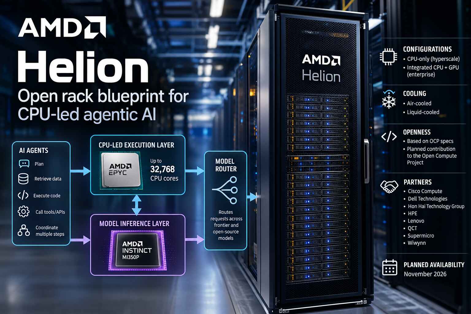
AMD unveils open Helion rack blueprint for CPU-led agentic AI, but the performance questions remain
The AI supercomputer’s hidden bottleneck: GlobalFoundries joins TSMC’s packaging supply chain
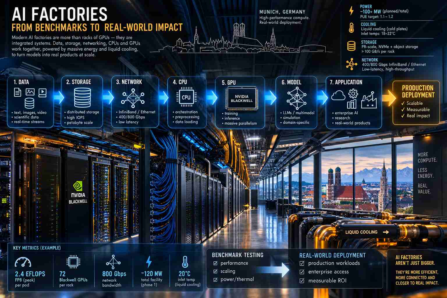
The AI factory becomes the new supercomputer test lab
previous arrow
previous arrow
next arrow
next arrow
 
Shadow
The AI supercomputer’s power problem is moving inside the rack: Delta pushes 800 VDC toward NVIDIA’s next generation
Featured

The AI supercomputer’s power problem is moving inside the rack: Delta pushes 800 VDC toward NVIDIA’s next generation

Deckard, Staff Editor October 15, 2026, 12:00 pm

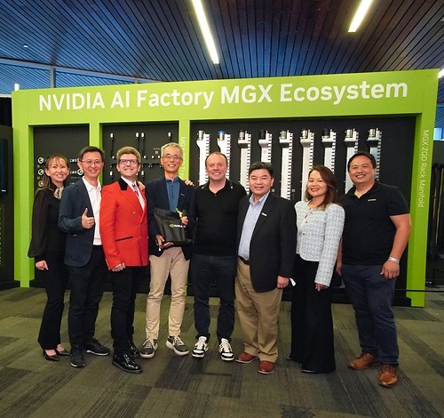
The race to build more powerful AI supercomputers is forcing a fundamental redesign of the electrical infrastructure that feeds them. At the Open Compute Project (OCP) Global Summit 2026, Delta Electronics is showcasing an increasingly comprehensive portfolio of high-voltage direct-current power delivery and liquid-cooling systems designed for the next generation of NVIDIA-based AI infrastructure.

The announcement highlights a problem that is becoming harder to ignore as accelerator systems scale toward megawatt-class racks: delivering electricity to the processors efficiently is no longer a peripheral data-center engineering task. It is becoming a central constraint on how much computing capacity operators can deploy within a given footprint, power envelope, and cooling budget.

Delta’s portfolio includes an 800 VDC in-row power rack rated for 660 kilowatts, a 90 kW DC/DC power shelf, a solid-state transformer designed to convert medium-voltage AC directly to 800 VDC, high-current power distribution hardware and a liquid-to-liquid coolant distribution unit rated for up to 2.5 megawatts of cooling capacity. The company says these systems are intended to support NVIDIA Vera Rubin NVL72 platforms and other systems built around NVIDIA’s MGX modular server architecture.

The engineering direction is significant. The commercial implications, however, remain less certain: Delta’s latest announcement is primarily a showcase of an existing product portfolio, not evidence of a new NVIDIA contract, a confirmed customer deployment, or independently verified data-center efficiency gains.

Why AI supercomputers are outgrowing conventional power delivery

The underlying challenge is electrical distribution at extreme power densities.

As AI infrastructure evolves from racks consuming tens of kilowatts toward configurations drawing hundreds of kilowatts and eventually approaching a megawatt, traditional power-delivery architectures become increasingly difficult to scale. More current must travel through conductors, more conversion equipment occupies valuable rack space, and electrical losses generate additional heat that cooling systems must remove.

At a given power level, increasing distribution voltage reduces the current required to deliver that power. For a simplified DC system, the relationship is:

[ P=VI ]

where (P) is electrical power, (V) is voltage, and (I) is current.

Delivering 1 megawatt at 54 volts requires approximately 18,519 amperes. At 800 volts, the same power requires approximately 1,250 amperes. These figures assume idealized DC delivery at the stated voltage and exclude conversion losses and differences in the electrical distribution topology.

That is a substantial reduction in current. Because resistive losses in a conductor scale with the square of current, increasing voltage can dramatically reduce distribution losses when conductor resistance and delivered power are held constant.

The benefits extend beyond electrical efficiency. Higher-voltage distribution can reduce conductor cross-sections, simplify buswork, and free space otherwise occupied by power equipment. In a densely packed AI rack, that space can be valuable for accelerators, memory, networking and cooling hardware.

But higher voltage does not eliminate engineering complexity. It shifts the challenge toward insulation, protection, conversion electronics, connectors, fault isolation, and safe maintenance. The practical benefits depend on the complete electrical design rather than voltage alone.

Delta’s grid-to-rack strategy

Delta is positioning itself to supply more than individual power components. Its portfolio spans several stages of the infrastructure between the incoming electrical supply and the computing hardware.

The company's 800 VDC in-row power rack is rated for 660 kW of output and incorporates 480 kW of battery backup capacity. Delta also lists a compact 800 kW variant without an integrated battery backup unit. The rack-level system is designed to consolidate power conversion and backup functions around high-density AI infrastructure.

A separate 90 kW DC/DC power shelf converts 800 VDC to a lower-voltage distribution rail. Delta’s announcement describes a 50 V output, while its broader product materials also discuss a 54 V implementation. Those output configurations should not be treated as interchangeable without confirming the specifications of the particular product and system design.

The distinction matters because the power architecture must accommodate the requirements of the rack, intermediate conversion stages, and the final voltage-regulation circuitry serving individual processors.

Delta is also presenting a solid-state transformer intended to convert medium-voltage AC directly to 800 VDC. Conventional architectures often involve multiple conversion stages between the utility supply and the computing load. Integrating conversion functions could reduce equipment footprint and losses, although actual performance will depend on operating conditions and the implementation.

The company's high-voltage DC power-distribution board and a 5,000-ampere liquid-cooled busbar extend the design into the distribution system itself. The busbar is intended for third-generation NVIDIA MGX racks, where high-current delivery and thermal management increasingly intersect.

Taken together, these components represent an attempt to engineer the power path as a coordinated system rather than a collection of independently optimized products.

That systems-level approach is increasingly important in AI infrastructure. Improving one power shelf's efficiency has limited value if losses elsewhere in the facility, inadequate protection, or cooling constraints prevent the entire installation from operating at its intended capacity.

Megawatt-class cooling becomes part of the electrical equation

Electrical distribution is only half the challenge. Nearly all the power consumed by computing hardware ultimately becomes heat that must be removed.

Delta's 800 VDC liquid-to-liquid coolant distribution unit is rated for up to 2.5 MW of cooling capacity, placing it in the same broad capacity class as competing systems being presented at the summit. The company is also highlighting cold-plate technology for NVIDIA Vera Rubin NVL72 systems.

Liquid cooling allows heat to be captured close to the processors and transferred into a circulating coolant loop. A coolant distribution unit manages the interface between the facility's cooling infrastructure and the equipment-side liquid circuit, helping control flow, pressure and heat transfer.

At these power levels, cooling is not simply a matter of installing larger pumps. Operators must account for flow distribution, coolant chemistry, filtration, pressure drop, leak detection, redundancy and the consequences of component failure. The facility's ability to reject heat also places demands on chillers, heat exchangers, water systems or other heat-rejection equipment.

Power and cooling must therefore be engineered together. A rack that can receive hundreds of kilowatts electrically is not useful if its thermal infrastructure cannot continuously remove the corresponding heat.

The same principle applies to energy efficiency. Higher electrical conversion efficiency can reduce wasted energy, but total facility performance depends on the entire system, including cooling power, pumps, fans, power distribution and the computing workload itself.

The 800 VDC transition is not yet a single settled standard

The industry's move toward higher-voltage DC distribution is gaining momentum, but describing 800 VDC as one universally established standard would be premature.

Delta's products use a two-wire 800 VDC architecture. The Open Compute Project's Diablo 400 specification, developed with participation from Google, Meta, and Microsoft, uses a three-wire arrangement with positive and negative 400-volt rails, producing 800 volts between the outer rails.

Both approaches address the challenge of distributing power to high-density computing systems, but their electrical arrangements are not identical. Compatibility depends on the relevant specifications, equipment interfaces, and system design.

Safety and protection also require attention. High-voltage DC systems present demanding arc-interruption and fault-management challenges. The industry must establish and implement suitable protection practices, equipment standards and installation requirements as deployments expand.

For data-center operators, the question is not simply whether 800 VDC can deliver power more efficiently. It is whether equipment from different vendors can work together reliably, whether operators can maintain it safely, and whether the architecture can be supported at commercial scale.

Those questions are especially important for facilities expected to operate continuously under variable AI workloads.

NVIDIA's projected gains need to be treated as targets

The broader NVIDIA 800 VDC architecture has been associated with projections of 45% less copper, up to 5% better end-to-end power efficiency, and up to 70% lower maintenance requirements.

These figures are projections for the planned architecture, not measured results from a production AI data center. They should not be interpreted as demonstrated savings from Delta's newly showcased hardware.

Delta's own component specifications also require context. Its power systems advertise peak conversion efficiencies reaching approximately 98% or more, depending on the component and configuration. Those figures are vendor specifications, with the relevant operating points and test conditions not fully disclosed in the announcement.

Peak efficiency is useful for comparing technology under defined conditions, but it does not describe performance across an entire facility. Power conversion equipment can behave differently at partial load, during rapid changes in demand, and under varying temperatures.

For AI systems, the operating profile matters. Training and inference workloads can create changing power demands, and infrastructure must maintain stability while responding to those variations.

A credible evaluation would require measured efficiency curves, thermal performance, reliability data, and end-to-end results under representative operating conditions. Ideally, those measurements would cover the complete path from incoming power to the computing load.

Without such evidence, the announced numbers remain engineering targets and product specifications rather than proof of operational savings.

Delta faces a crowded race to supply the next AI infrastructure generation

Delta is not the only company preparing hardware for the transition.

Lite-On is presenting competing high-voltage power-conversion and liquid-cooling products. Navitas is targeting power-conversion components for NVIDIA MGX systems, while Vertiv, Eaton and Schneider Electric are developing or promoting their own approaches to high-voltage distribution and next-generation AI infrastructure.

The competitive landscape reflects a broader change in the AI hardware market. As accelerator performance increases, differentiation increasingly depends on everything surrounding the processor: power conversion, thermal management, networking, mechanical design, and the ability to deploy complete systems at scale.

Delta's potential advantage is breadth. Its portfolio extends from solid-state transformers and power distribution to rack-level power systems, cooling equipment and microgrid solutions. That could simplify integration for customers seeking a coordinated infrastructure design.

Yet a broad product portfolio does not automatically establish market leadership. Customers will also evaluate delivery schedules, manufacturing capacity, field reliability, service support, interoperability, and total cost of ownership.

The critical milestone is not how many components a company can display at a conference. It is how many can be delivered, integrated, qualified, and operated successfully in production environments.

The real deadline is commercial deployment

The timing of the 800 VDC transition is closely linked to the next generation of high-density AI systems, including NVIDIA's planned Kyber-era infrastructure for 2027. The architecture is intended to support racks whose power demands exceed what conventional rack-level distribution can accommodate economically.

That creates a race for suppliers. Power systems, connectors, busbars, protection equipment and liquid-cooling infrastructure must mature alongside the computing platforms they are intended to support.

For operators planning new AI facilities, the decision will involve more than purchasing compatible racks. They must consider electrical distribution from the facility perimeter, backup power, cooling capacity, physical layout, maintenance procedures, and future expansion.

Retrofitting existing data centers introduces additional complications. An architecture that makes sense for a purpose-built AI factory may not be economically justified for a conventional enterprise facility with lower rack densities or a different workload mix.

The transition is therefore likely to be driven first by AI-dense deployments where the space and efficiency benefits are most valuable, rather than by a wholesale conversion of every data center.

Delta's announcement does not identify new customer deployments, contracted volumes or a confirmed production installation resulting from the latest showcase. Those omissions limit what can be concluded about commercial adoption.

A meaningful engineering shift, not yet a proven infrastructure breakthrough

Delta's presentation at the OCP Global Summit underscores how the escalating performance demands of the AI industry are necessitating a fundamental redesign of electrical and thermal infrastructure.

The industry's shift toward 800 VDC architectures offers the potential to reduce current requirements, minimize copper usage, and streamline conversion complexity, thereby optimizing space for high-density computing components. By integrating power delivery with megawatt-class liquid cooling, operators may be better positioned to design facilities tailored to the specific requirements of next-generation accelerators, moving beyond the limitations of conventional infrastructure.

However, the success of this transition relies on more than just promising technical specifications. It will require the maturation of competing electrical architectures, the standardization of safety and maintenance protocols, and rigorous, real-world validation of performance under diverse, high-load workloads.

While Delta has introduced a robust portfolio addressing critical infrastructure challenges, the industry has yet to reach a definitive consensus on a single implementation, nor have the projected efficiencies been fully realized in production environments. Moving forward, the true viability of these advancements will be determined by deployment milestones, customer adoption, interoperability benchmarks, and transparent, independently verified performance data. Ultimately, the next evolution of AI supercomputing hinges as much on the capacity to safely and efficiently manage massive power and thermal loads as it does on the speed of the processors themselves.

GlobalFoundries’ $21B chip deal targets America’s AI infrastructure
Featured

GlobalFoundries’ $21B chip deal targets America’s AI infrastructure

CHRIS O'NEAL, PUBLISHER October 15, 2026, 10:00 am

Japan will fund two planned fabs, while separate U.S. funding supports advanced packaging and silicon photonics, technologies increasingly important to AI and HPC systems.

Under a U.S.-Japan initiative valued at up to $21 billion, GlobalFoundries is slated to operate two semiconductor fabrication facilities in Malta, New York. While Japan provides the necessary capital, the construction of the second facility remains contingent upon future market demand. Concurrently, a separate, perhaps more immediate strategic development for the AI and high-performance computing (HPC) sectors involves the reallocation of up to $955 million in existing CHIPS Act funding. These funds will be directed toward advancing packaging, silicon photonics, and silicon-germanium technologies.

It is critical to distinguish between these two initiatives: the new fabs are designed for foundational semiconductor production rather than leading-edge AI processors, whereas the packaging investment addresses the increasingly vital challenge of data movement and chip connectivity as AI systems scale.

Collectively, these agreements reflect a strategic effort to enhance U.S. semiconductor capacity; however, the extent to which they alleviate supply-chain constraints will depend on production timelines, customer commitments, and actualized capacity. The headline figure of $21 billion warrants closer scrutiny, as the initial investment is approximately $10 billion, with the second phase tied to market conditions. Furthermore, GlobalFoundries will operate the facilities as a technology provider rather than as the owner. 

Simultaneously, the reallocation of $955 million to GlobalFoundries’ existing facilities in Malta and Burlington, Vermont, carries significant implications for the supercomputing industry. As AI systems scale, performance is increasingly dictated by the technologies that manage data transmission between processors, memory, and networking systems. Consequently, these announcements represent two distinct but complementary investments: one focused on expanding foundational manufacturing, and the other on strengthening the bandwidth and connectivity infrastructure essential for future AI and HPC systems.

The supercomputer is more than its processors

The semiconductor industry has spent years concentrating on accelerator performance, transistor density, and the race to develop increasingly powerful AI processors. Yet the largest computing systems face a broader engineering challenge.

An accelerator can perform enormous numbers of calculations, but its practical contribution to a distributed workload depends on how quickly data reaches it, how efficiently results move between devices, and how effectively the surrounding system manages power and heat.

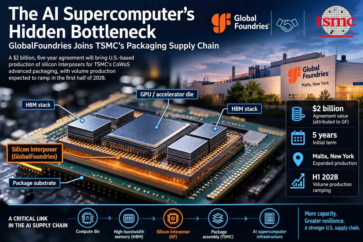
Advanced packaging has become central to this problem. Modern high-performance processors can combine multiple compute and memory components within tightly integrated packages. Silicon interposers provide dense connections between dies, enabling the high-bandwidth interfaces required by complex multi-die designs.

These components do not independently make a processor faster. Their value comes from enabling the integration and data movement that a high-performance architecture requires.

GlobalFoundries' separate agreement with Taiwan Semiconductor Manufacturing Co. (TSMC), announced October 8, illustrates the point. The companies announced a multiyear agreement valued at $2 billion under which GlobalFoundries will manufacture silicon interposers for TSMC's Chip-on-Wafer-on-Substrate (CoWoS) advanced-packaging ecosystem. GlobalFoundries expects production to ramp in the first half of 2028.

The arrangement establishes a planned U.S.-based manufacturing source for an important component of advanced AI packaging. It does not, however, mean that GlobalFoundries will manufacture TSMC's leading-edge AI processors or perform every stage of final assembly and packaging.

That distinction matters. A domestic source of interposers can strengthen one part of the supply chain without eliminating dependence on other manufacturers, packaging operations or specialized equipment.

For HPC system designers, the practical question is whether the additional capacity will deliver the components, yields, manufacturing consistency and production volumes needed to support increasingly complex accelerator systems.

The announcement establishes an industrial objective. It does not yet provide enough public information to quantify the resulting improvement in AI-system performance or supply availability.

Silicon photonics and the interconnect challenge

The $955 million federal award reallocation targets another increasingly important part of the computing stack: moving data efficiently between devices.

Silicon photonics uses optical technology to transmit information, while silicon-germanium technologies support specialized semiconductor applications, including high-frequency electronics. Both are relevant to communications infrastructure and data-center systems.

As accelerator clusters grow, communication networks must move increasing quantities of data between compute nodes and across the broader facility. Electrical interconnects remain essential, but their power consumption, reach, and bandwidth constraints create pressure to develop more efficient optical technologies.

Near-packaged optics and co-packaged optics are among the approaches being developed to bring optical connectivity closer to switching or computing silicon. Their potential benefits include improved bandwidth density and reduced energy consumed by portions of the data-movement infrastructure.

Those benefits are not automatic. They depend on the implementation, optical components, packaging approach, thermal characteristics, manufacturing yield, and system-level design.

GlobalFoundries has already described its silicon-photonics work as part of a broader effort to support next-generation AI and HPC connectivity. Its existing capabilities in Malta and Burlington will receive investment under the amended federal award.

The critical point is that the $955 million is not a new federal award added on top of the existing CHIPS funding. The Commerce Department is reallocating up to that amount from GlobalFoundries' existing $1.5 billion award. GlobalFoundries has agreed to increase its own capital investment in the facilities covered by the amendment to $5 billion.

Commerce says the revised allocation will support technologies increasingly important to data centers and communications infrastructure.

What remains unclear is how quickly the investments will translate into high-volume production, which specific technologies will reach commercial maturity first, and how much capacity will be available to customers building large AI systems.

The $21 billion headline needs qualification

The proposed fabs represent a substantial manufacturing expansion, but the financial structure deserves more careful examination than a headline announcing a $21 billion investment might suggest.

Japan will provide the capital for the two facilities. The initial project involves approximately $10 billion and is expected to begin operations in 2029. The additional approximately $10 billion associated with the second facility depends on a decision expected before the end of 2028, tied to market demand.

The combined target is approximately 900,000 300-millimeter wafers of annual capacity per fab when fully operational. If both facilities proceed and reach their stated capacity, the initiative could add approximately 1.8 million wafers of annual capacity.

Those figures are targets, not current production. Nor do they establish how much usable semiconductor output will result, which products will be manufactured at particular process nodes, or how much capacity individual customers will secure.

GlobalFoundries describes the new facilities as foundational semiconductor production intended to support automotive, industrial and connected-infrastructure markets. The company has not disclosed the specific process nodes for the two fabs.

They should therefore not be presented as new leading-edge AI-processor factories.

The business model also differs from a conventional expansion financed and owned by the manufacturer. GlobalFoundries will act as technology provider and operator, earning construction-management fees, ongoing operating fees and technology-licensing revenue.

The company expects approximately $50 million in construction-management revenue in 2027. It has also indicated that its fee-generating relationship with the facilities is intended to extend for at least 20 years.

That arrangement could give GlobalFoundries a long-term revenue stream without requiring it to own the facilities. But the available disclosures do not quantify the full expected operating and licensing economics, the ultimate profitability of the projects, or the risks associated with executing the manufacturing ramp.

The financial distinction is important: The total project funding is not equivalent to revenue for GlobalFoundries, and neither figure should be confused with profit.

Washington becomes a shareholder

The Japan-funded fab initiative also arrives alongside a separate change in the U.S. government's relationship with GlobalFoundries.

Under another agreement, the Commerce Department will receive an equity stake of approximately 4% in the company. GlobalFoundries CEO Tim Breen has separately described total U.S. government ownership as approximately 7%.

The precise terms of the new equity arrangement, including the purchase price, voting rights, board representation and exit provisions, have not been fully disclosed in the materials available for this report. The reported total ownership figure also requires reconciliation against the previously disclosed government equity positions.

These questions matter because government equity creates a different relationship from a conventional grant. Taxpayers may participate in the company's financial upside, but the public also needs clarity about the terms, governance, and objectives of that participation.

The fab arrangement introduces another layer. Japan supplies the capital for facilities that GlobalFoundries operates, while the U.S. and Japanese sides participate in the investment's ownership and financial returns.

Under the reported structure, available free cash flow is divided equally between the U.S. and Japan until a specified allocation threshold is reached, after which 90% goes to the U.S. Japan is expected to recover its principal and interest first.

The full terms, including the threshold and the precise governance arrangements, remain important unanswered questions.

The structure reflects a wider policy experiment: using international capital and public-sector participation to expand domestic industrial capacity while seeking financial returns for the participating governments.

Whether that model becomes a durable template for semiconductor infrastructure will depend on its execution, its economics and the extent to which the resulting facilities deliver the strategic capabilities promised.

The demand question cannot be ignored

GlobalFoundries expects the initiative to support demand across automotive, industrial and connected-infrastructure markets. The company's announcement also identifies Renesas Electronics and Apple as initial customers or customer interests, but public disclosures do not establish firm production volumes or detailed offtake terms.

Those distinctions matter when evaluating a manufacturing expansion of this scale.

Semiconductor factories are long-lived assets that require substantial investment, specialized equipment, skilled workers, and sustained utilization. Building capacity ahead of demand can provide supply-chain resilience, but it can also create financial pressure if customer requirements do not develop as anticipated.

The second fab's conditional status acknowledges that risk. GlobalFoundries' leadership has indicated that the company will not proceed if the market is insufficient.

For policymakers, that raises a central question: how should strategic capacity be valued when its benefits include supply-chain resilience and national security, but its commercial returns depend on future demand?

For HPC operators, the question is more immediate. Will the new facilities and the separate advanced-packaging investments deliver components that are difficult to obtain today, or will they primarily expand capacity in semiconductor categories that do not directly address the most acute constraints in AI infrastructure?

The answer will depend on the products, customers, and production schedules that emerge from the projects.

Three timelines, not one

The announcements also involve distinct schedules that should not be conflated.

The GlobalFoundries-TSMC silicon-interposer agreement targets a production ramp in the first half of 2028. The first Japan-funded fab is expected to begin operating in 2029. The separate photonics, SiGe, and advanced-packaging expansion under the amended CHIPS award does not have a single publicly specified completion date in the announcement.

The interposer manufacturing expansion is associated with GlobalFoundries' existing Malta campus, not simply with the two proposed Japan-funded fabs. Nor does the 2029 timeline for the new facilities establish that they will manufacture the components covered by the TSMC agreement.

This is more than a scheduling detail. Semiconductor supply chains depend on coordination between wafer production, packaging, testing, component qualification, and final system integration. A facility coming online does not mean every part of the surrounding supply chain will be ready at the same time.

The industry will need evidence of completed equipment installation, qualified processes, customer acceptance and reliable production before projected capacity can be treated as operational supply.

What the deal must prove

The expansion led by GlobalFoundries represents a significant development in the broader effort to fortify U.S. semiconductor manufacturing. The integration of Japanese capital, established manufacturing expertise, and targeted public investment has the potential to enhance critical capabilities for future computing and communications systems.

The long-term impact of these initiatives hinges on meeting development timelines, aligning capacity with market demand, and achieving cost-effective, high-yield production in advanced packaging and silicon photonics.

Furthermore, the company and relevant government agencies must provide greater transparency regarding process technologies, customer commitments, equity terms, and the structural relationship between public funding and private commercial agreements. Descriptions of the planned interposer capacity as the inaugural U.S.-based source for advanced packaging should be viewed with precise qualification; official government endorsements do not serve as independent technical verification of competitive market capabilities.

For the supercomputing trade, the broader implication is that the AI infrastructure race cannot be evaluated solely through announced investments or production volumes. Success must be measured by the operational capacity to manufacture, interconnect, and deploy the essential components required for large-scale computing systems.

The $21 billion initiative is a substantial strategic bet on semiconductor capacity. Its actual significance for AI and high-performance computing will depend on whether this output, bolstered by investments in photonics and advanced packaging, effectively alleviates existing constraints within the computing supply chain. Until production timelines, customer commitments, and financial terms are further clarified, this agreement should be viewed as a major industrial commitment whose technical and economic efficacy remains to be proven.

Microsoft’s Maia 300 promises 40% more AI tokens per megawatt; the benchmark is missing
Featured

Microsoft’s Maia 300 promises 40% more AI tokens per megawatt; the benchmark is missing

CHRIS O'NEAL, PUBLISHER October 13, 2026, 1:30 pm

While Microsoft’s third-generation inference accelerator offers a significant improvement in memory bandwidth and a dense 96-chip rack architecture, advancing the company’s objective to reduce reliance on third-party GPUs, its headline efficiency claims remain unverified. Furthermore, with production deployments not anticipated until 2027, the ambitious transition to a million-chip scale introduces substantial uncertainties regarding manufacturing capacity, power consumption, and economic viability.

Microsoft’s objective to transition toward proprietary silicon for AI infrastructure is exemplified by the introduction of the Azure Maia 300. By integrating high-bandwidth HBM4 memory, a multi-chiplet configuration, and a sophisticated rack-scale architecture, the system is engineered to address the complexities of modern inference workloads.

However, the headline assertion that the Maia 300 delivers 40% greater token efficiency per megawatt compared to leading GPU-based systems lacks necessary transparency. Microsoft has not disclosed the specific competing hardware, the underlying model architectures, the workload configurations, or the benchmark methodologies employed. Consequently, this claim remains a prospective projection rather than an independently verified performance metric.

In a market where performance-per-watt has become a critical benchmark for AI infrastructure, such distinctions are vital. Meaningful efficiency comparisons require standardized workloads, consistent service-level requirements, and clearly defined measurement boundaries. While the Maia 300 presents a compelling architectural design and a robust deployment roadmap, the validity of its efficiency advantages remains subject to future empirical validation.

The real advance may be memory, not arithmetic

Microsoft’s Maia 300 design reflects a growing challenge in large-scale AI inference: generating tokens efficiently can depend as much on moving data as on performing mathematical operations.

During autoregressive generation, a model repeatedly executes operations involving its weights and intermediate state. The key-value cache, or KV cache, stores attention-related information from previously processed tokens so that the model does not have to recompute the entire sequence for every new token. As context lengths grow and conversations involve multiple reasoning steps, memory capacity, bandwidth, and data movement can become critical constraints.

An accelerator with impressive peak arithmetic throughput can still underperform if its compute units spend too much time waiting for data.

Maia 300 appears designed to address that problem precisely.

According to specifications, the accelerator moves from Maia 200’s monolithic design to a multi-chiplet package. The compute die uses TSMC’s N2P process, while separate memory-controller and I/O chiplets use 3-nanometer technology. The division allows Microsoft to concentrate its most advanced process technology on the compute components while using different manufacturing technology for supporting functions.

The chip also introduces a non-uniform memory access architecture, intended to improve the placement of data relative to the compute resources that consume it. Microsoft describes software-defined dataflow, AI-assisted kernel optimization and enhanced support for low-precision MXFP4 operations as additional tools for reducing data movement and improving resource utilization.

These are meaningful design choices. They are not, by themselves, proof of a particular end-to-end performance advantage.

The specifications show why memory deserves the attention.

Maia 300 is listed with 288 GB of HBM4 across eight stacks and peak memory bandwidth of 18 TB/s. Maia 200 has 216 GB of HBM3e across six stacks and 7.1 TB/s of bandwidth.

That represents approximately 2.54 times the memory bandwidth and 33% more memory capacity. Based on the published figures, peak memory bandwidth per watt rises from approximately 9.5 GB/s per watt on Maia 200 to 18.9 GB/s per watt on Maia 300.

In other words, the new generation more than doubles this particular measure of memory bandwidth efficiency.

Peak compute throughput improves less dramatically. Microsoft lists 13.8 petaflops at FP4 and 6.9 petaflops at FP8 for Maia 300, compared with 10.1 petaflops at FP4 and 5.1 petaflops at FP8 for Maia 200. Those figures represent gains of approximately 37% and 35%, respectively.

But listed chip power also increases, from 750 watts to 950 watts. Dividing the published peak FP4 throughput by chip power produces an approximate 8% improvement in peak FP4 throughput per watt.

These calculations are derived from vendor specifications, not measured application benchmarks. They also do not account for differences in utilization, numerical precision, memory traffic, or software efficiency.

Nevertheless, the contrast is revealing: Maia 300’s greatest numerical improvement is in memory bandwidth, not compute throughput per watt.

That is a plausible design strategy for inference workloads dominated by data movement. The next question is how consistently that architectural advantage translates into more completed tokens under real production conditions.

The 40% efficiency claim needs a benchmark

Microsoft’s headline figure is potentially important because electricity is becoming a major constraint on the expansion of AI infrastructure.

If an accelerator platform can genuinely generate 40% more useful tokens per megawatt than a competing system while meeting the same latency, quality and availability requirements, the implications could extend beyond electricity costs. Better throughput within a fixed power allocation can increase the number of AI services a data center supports without requiring an equivalent increase in electrical capacity.

But the phrase tokens per megawatt is not a complete benchmark specification.

Which model is being served? What are its parameter count, precision, and context length? How many concurrent requests are processed? What batch sizes are used? What are the input-to-output token ratios? What latency limits must be met? Are the systems compared at equivalent output quality and reliability?

These details can change the result substantially.

Aggressive batching, for example, can improve accelerator utilization and throughput, but may increase waiting time for individual requests. A configuration optimized for maximum throughput may therefore be unsuitable for an interactive assistant that must respond quickly. Conversely, a low-latency configuration may sacrifice aggregate throughput to meet response-time targets.

The comparison also needs to define its power boundary. Accelerator power alone is not the same as total rack power, and rack power is not the same as facility power. Host CPUs, networking, memory, cooling and power-conversion losses all influence the amount of useful inference a data center can deliver per megawatt of electrical capacity.

Microsoft’s announcement describes a complete system rather than just a chip, which is the correct level at which to consider performance. But the public 40% claim does not identify enough benchmark detail to establish how the comparison was conducted.

Nor is the claim independently reproducible today. Maia is deployed within Microsoft’s own infrastructure strategy, and the announcement does not establish a generally available Maia 300 instance through which outside researchers could run an equivalent test.

The proper conclusion is not that Microsoft’s number is necessarily wrong. It is that readers cannot yet determine precisely what it means or independently verify it.

The distinction is especially important because Maia 300 will not begin production deployments until 2027. By then, the relevant competition will have evolved. Microsoft’s results must ultimately be assessed against the GPU and custom-accelerator platforms available when Maia 300 actually enters service, rather than against an unspecified snapshot of today’s hardware.

Seven times the rack throughput is not seven times the efficiency

Microsoft also advertises up to seven times the rack-scale token throughput of Maia 200. That figure sounds extraordinary until the system configurations are examined.

The published Maia 300 configuration contains 96 accelerators in a rack rated at approximately 167 kilowatts. Maia 200’s comparison rack contains 48 accelerators and draws approximately 64 kilowatts.

Maia 300 therefore doubles the accelerator count while increasing rack power by approximately 2.6 times.

The comparison is not meaningless. A denser rack with substantially greater aggregate memory bandwidth can be valuable when a data center’s constraints include floor space, interconnect topology, and the ability to serve larger workloads. But a sevenfold throughput figure should not be confused with a sevenfold improvement in efficiency.

Normalizing the advertised rack throughput by the stated power figures produces a much smaller relative gain than the raw rack comparison. Microsoft’s claimed Maia 300 per-watt advantage over Maia 200 is approximately 2.5 times.

That is still a substantial claim, but it is a different claim.

External comparisons require similar discipline. Reuters reported that Nvidia’s GB300 rack configuration contains 72 GPUs and draws approximately 142 kilowatts. Maia 300’s 96-accelerator rack has a higher stated power demand, but accelerator count and rack power alone cannot establish which system delivers better inference performance.

The systems must be evaluated on comparable models, precision, throughput, latency, utilization, and power boundaries.

For HPC engineers, the distinction between peak rack throughput and useful work per unit of energy is fundamental. A large system can deliver more aggregate output simply by consuming more power and deploying more silicon. The engineering challenge is to demonstrate how much additional useful work it delivers for every additional unit of electricity and capital investment.

A 167-kilowatt rack changes the infrastructure equation

Maia 300 is also a data-center infrastructure story.

Microsoft’s announced rack configuration contains 96 accelerators, 27.6 TB of aggregate HBM capacity and approximately 1.7 PB/s of aggregate HBM bandwidth. The rack’s stated power envelope is 167 kW.

That is roughly 1.74 kW per accelerator slot when rack-level power is divided by the accelerator count. It is not the power consumption of an individual Maia 300 chip: the accelerator itself is rated at 950 watts, and the rack figure includes other system components.

The cooling design combines liquid cooling for accelerators, voltage regulators and switch ASICs with air cooling for the remaining components. Microsoft says the systems can also operate in older air-cooled data centers, although that statement should not be interpreted as a guarantee that every existing facility can accommodate the rack’s power density without electrical, thermal or mechanical modifications.

The in-rack fabric uses six switch ASICs across three liquid-cooled trays, with an optical second tier connecting up to 128 racks into a larger superpod. Microsoft also describes a two-tier Ethernet-based scale-up fabric, custom AI transport, and 32 ports operating at 400 Gb/s.

These details matter because inference at scale is not simply a matter of installing faster chips. Data must move between memory and compute resources, across accelerators and between racks without allowing communication overhead to erase the benefits of additional silicon.

The challenge becomes more demanding for long-context reasoning and multi-step agentic workloads, where requests can require repeated model execution, sustained KV-cache access and communication among distributed resources.

Microsoft’s system-level approach is technically sensible. Yet the 167-kW rack rating also underscores the scale of the deployment challenge. Better efficiency per token does not eliminate the need to secure power, cooling capacity, networking and physical space for a much larger fleet.

The million-chip question

Microsoft says it intends to scale its Maia family to multigigawatt deployments beginning in 2027. Reuters has reported the possibility of more than one million Maia 300 chips being deployed next year, while earlier trade reporting described discussions involving more than 300,000 units for 2027 delivery.

Those figures should not be treated as equivalent production commitments. Microsoft has not publicly reconciled them in the announcement.

The difference is material.

At 96 accelerators per rack, one million chips would require approximately 10,417 racks. At 167 kW per rack, that represents about 1.74 GW of rack power alone.

A 300,000-chip deployment would correspond to approximately 3,125 racks and 522 MW at the same stated rack power.

These are derived estimates based on the published rack configuration. They exclude additional facility overhead and should not be interpreted as confirmed deployment plans.

The scale of the arithmetic illustrates why a shipment forecast cannot be separated from data-center construction and power procurement. Even if the silicon can be manufactured on schedule, a deployment of this magnitude requires facilities capable of receiving, powering, cooling and networking the equipment.

Manufacturing is another constraint. Maia 300 depends on advanced compute-die manufacturing, HBM4 supply, and sophisticated packaging. Those inputs are also important to other AI accelerator vendors competing for foundry capacity, memory and packaging resources.

The chiplet design may offer manufacturing and cost advantages, but the announcement does not establish how much capacity has been secured, what yields Microsoft expects, or how much flexibility it has if any major component becomes a bottleneck.

Microsoft’s broader capital expenditure plans demonstrate the company’s commitment to AI infrastructure. They do not, on their own, establish that a particular accelerator will ship in a particular quantity on a particular date.

The production timeline must therefore be treated as a milestone to watch, not a completed deployment.

Microsoft’s strategic objective is bigger than one chip

The most consequential part of the announcement may be Microsoft’s intention to make Maia its primary inference system for Microsoft products and services.

That ambition would change the company’s relationship with the accelerator market. Rather than relying principally on external vendors for the silicon underpinning its own AI services, Microsoft would have greater control over the hardware, systems software, networking and workload-specific optimizations that determine inference economics.

The Maia 200 production program provides some evidence that the strategy is progressing beyond laboratory development. Microsoft says Maia 200 is serving production workloads, including Copilot, and supports OpenAI models, Microsoft’s own MAI models and open-source model families. GitHub Copilot and Microsoft Foundry were identified as intended additions to its Maia deployment plans.

That operating experience gives Maia 300 a more credible foundation than a first-generation chip announcement.

It also raises a question Microsoft has not yet answered clearly: how will customers access the new hardware?

The announcement does not establish that Azure customers will be able to select Maia 300 as a generally available accelerator instance or run their own models directly on it through Microsoft Foundry. Internal use by Microsoft’s services and broad customer access are different propositions.

A successful internal accelerator can still be strategically valuable, even if customers never interact with it directly. Microsoft could optimize its own services, manage its infrastructure costs and reserve purchased GPUs for workloads better suited to them.

But claims about a transformed cloud computing market would require evidence beyond the announcement of a new chip.

There is also an economic question. Microsoft emphasizes performance per megawatt, but the public announcement does not provide a comparable Maia 300 tokens-per-dollar figure. Electricity is important, but the total cost of inference also includes accelerators, hosts, networking, memory, cooling, facility construction, software engineering, and equipment utilization.

An accelerator that produces more tokens per unit of electricity is not automatically the least expensive system to operate.

The commercial test is whether Microsoft can deliver the required model quality and service levels at a lower total cost while deploying the hardware at the intended scale.

What Microsoft must demonstrate next

Microsoft has promised more information at its Ignite conference in November. That provides an opportunity to move the discussion from architectural claims to verifiable operating evidence.

Several questions deserve direct answers.

First, what GPU system, model, and serving configuration underpin the 40% efficiency expectation? A reproducible benchmark should specify precision, context length, batch size, throughput, latency, and the power boundary used.

Second, what does the 2027 deployment commitment mean in physical terms? Microsoft should clarify the difference between chips ordered, chips manufactured, systems installed and systems accepting production workloads. It should also explain the reported difference between the 300,000-unit figure and the possibility of more than one million chips.

Third, what is the actual deployment target in gigawatts, and which data centers will receive Maia 300 first? A power figure without a deployment schedule and identified capacity remains an incomplete description of the program.

Fourth, will customers gain direct access to Maia 300, or will Microsoft initially reserve it for first-party services?

Finally, how does Maia 300 compare on tokens per dollar and useful throughput per facility megawatt against the GPU systems Microsoft will continue to purchase? Those comparisons should include the alternative systems available when Maia 300 reaches production, not simply the generation available at announcement time.

The verdict: credible engineering, unproven economics

Maia 300 deserves serious attention from the supercomputing community. Its increased HBM capacity, substantially higher memory bandwidth, chiplet architecture, and integrated rack design address real challenges in large-scale inference.

Microsoft’s decision to optimize the entire platform around its own production workloads is also significant. At hyperscale, close coordination between models, kernels, compilers, memory systems, networking and silicon can yield advantages that isolated peak-performance specifications fail to capture.

But the announcement does not yet establish the size of those advantages in independently reproducible terms.

The 40% more-tokens-per-megawatt claim lacks a named comparator and a disclosed workload. The sevenfold rack-throughput figure combines a doubled accelerator count with a much higher power envelope. The multigigawatt ambition has no precise public target, and the competing chip-volume reports have not been reconciled.

None of those gaps invalidates Maia 300’s architecture. They define what remains to be demonstrated.

For Microsoft, the real test begins when production systems are installed, workloads are measured, and the economics can be compared against competing platforms. Until then, Maia 300 should be regarded as a technically substantial infrastructure program with promising design choices, not a proven 40% efficiency victory.

The chip may ultimately help Microsoft extract more useful AI work from every megawatt. The industry still needs the benchmarks, deployment data, and cost figures to establish how much.

  • AMD unveils open Helion rack blueprint for CPU-led agentic AI, but the performance questions remain
  • The AI supercomputer’s hidden bottleneck: GlobalFoundries joins TSMC’s packaging supply chain
  • 1
  • 2
Page 1 of 2
POPULAR RIGHT NOW
  • 10,000 AI agents, 130 billion tokens and 88 hours: How OpenAI turned Navier–Stokes into a supercomputing workload
    10,000 AI agents, 130 billion tokens and 88 hours: How OpenAI turned Navier–Stokes into a supercomputing workload
  • Jensen Huang to G20: Build the AI infrastructure, or risk being left behind
    Jensen Huang to G20: Build the AI infrastructure, or risk being left behind
  • Millions of CPU cores meet 69 billion molecules: AI rewrites the rules of computational drug discovery
    Millions of CPU cores meet 69 billion molecules: AI rewrites the rules of computational drug discovery
  • The algo is the supercomputer: AI rewrites the search for protein ion-binding sites
    The algo is the supercomputer: AI rewrites the search for protein ion-binding sites
  • Supercomputing rewrites the Sun’s history and Earth’s climate
    Schematic of the heliosphere. Several elements that form the heliosphere are noted. The width of the sector region is expected to vary with the solar cycle. Figure created by Adam Hong.
    Schematic of the heliosphere. Several elements that form the heliosphere are noted. The width of the sector region is expected to vary with the solar cycle. Figure created by Adam Hong.
  • Qualcomm enters the supercomputing arena as AWS partnership challenges Nvidia’s AI infrastructure dominance
    Qualcomm enters the supercomputing arena as AWS partnership challenges Nvidia’s AI infrastructure dominance
  • Fugaku goes inside the molecular machine: Supercomputer simulations reveal how kinesin knows which way to step
    Fugaku goes inside the molecular machine: Supercomputer simulations reveal how kinesin knows which way to step
  • From the Tibetan Plateau to California: Supercomputing reveals a hidden source of flood predictability
    From the Tibetan Plateau to California: Supercomputing reveals a hidden source of flood predictability
  • Supercomputing reconstructs the moon Venus may have lost
    Supercomputing reconstructs the moon Venus may have lost
  • Japanese supercomputer recreates the birth of the Universe’s monster black holes
    Visualization of the simulation by ATERUI III showing a rapidly growing black hole surrounded by gas. Red indicates areas of higher temperature. (Credit: Sunmyon Chon, Takaaki Takeda, 4D2U Project, NAOJ)
    Visualization of the simulation by ATERUI III showing a rapidly growing black hole surrounded by gas. Red indicates areas of higher temperature. (Credit: Sunmyon Chon, Takaaki Takeda, 4D2U Project, NAOJ)
THIS YEAR'S MOST READ
  • Wall Street wants to trade supercomputing power like oil
    Wall Street wants to trade supercomputing power like oil
  • Beamforming the future: BeammWave's 6G push signals the rise of orbital-terrestrial wireless networks
    Joakim Axmon
    Joakim Axmon
  • AI breaks conservation barriers: Australia’s Wildlife Observatory leverages supercomputing to protect biodiversity
    AI breaks conservation barriers: Australia’s Wildlife Observatory leverages supercomputing to protect biodiversity
  • Silicon spintronics brings the P-computer closer to reality
    Microscope image of a semiconductor-integrated spintronic test chip developed by researchers at Tohoku University and NIST. The device demonstrates the first silicon-integrated probabilistic bit (p-bit), a key building block for future large-scale probabilistic computers designed for AI and optimization workloads.
    Microscope image of a semiconductor-integrated spintronic test chip developed by researchers at Tohoku University and NIST. The device demonstrates the first silicon-integrated probabilistic bit (p-bit), a key building block for future large-scale probabilistic computers designed for AI and optimization workloads.
  • Hidden order, revealed at scale: Supercomputing, electron ptychography uncover the inner workings of relaxor ferroelectrics
    Hidden order, revealed at scale: Supercomputing, electron ptychography uncover the inner workings of relaxor ferroelectrics
  • Physics-trained ‘Digital Super Brain’ learns from supercomputers to accelerate discovery
    Physics-trained ‘Digital Super Brain’ learns from supercomputers to accelerate discovery
  • Memory has become the new compute: Why Micron, SK Hynix crossing $1 trillion matters to supercomputing
    Memory has become the new compute: Why Micron, SK Hynix crossing $1 trillion matters to supercomputing
  • Cosmic ambition at scale: UK’s supercomputer unlocks a 2.5 petabytes universe
    Cosmic ambition at scale: UK’s supercomputer unlocks a 2.5 petabytes universe
  • Huawei’s Tau Scaling ambition tests the limits of post-Moore semiconductor reality
    He Tingbo from HUAWEI delivered a keynote speech titled "New Semiconductor Path in Practice"
    He Tingbo from HUAWEI delivered a keynote speech titled "New Semiconductor Path in Practice"
  • Intel's Q1 results signal supercomputing surge driving Xeon momentum
    Intel's Q1 results signal supercomputing surge driving Xeon momentum
MOST READ OF ALL-TIME
  • Largest Computational Biology Simulation Mimics The Ribosome
    Details
    112750
    The amino acid (green) slithers into the chemical reaction center, moving through an evolutionarily ancient corridor of the ribosome (purple). The amino acid is delivered to the reaction core by the transfer RNA molecule (yellow).
    The amino acid (green) slithers into the chemical reaction center, moving through an evolutionarily ancient corridor of the ribosome (purple). The amino acid is delivered to the reaction core by the transfer RNA molecule (yellow).
  • Silicon 'neurons' may add a new dimension to chips
    Details
    82231
    Silicon 'neurons' may add a new dimension to chips
  • Linux Networx Accelerators Expected to Drive up to 4x Price/Performance
    Details
    76251
  • Complex Concepts That Really Add Up
    Details
    74777
    Complex Concepts That Really Add Up
  • Blue Sky Studios Donates Animation SuperComputer to Wesleyan
    Details
    68820
    Each rack holds 52 Angstrom Microsystem-brand “blades,” with a memory footprint of 12 or 24 gigabytes each. (Photos by Olivia Bartlett Drake)
    Each rack holds 52 Angstrom Microsystem-brand “blades,” with a memory footprint of 12 or 24 gigabytes each. (Photos by Olivia Bartlett Drake)
  • Humanities, HPC connect at NERSC
    Details
    58696
  • TeraGrid ’09 'Call for Participation'
    Details
    55638
  • Turbulence responsible for black holes' balancing act
    Details
    53073
  • Cray Wins $52 Million SuperComputer Contract
    Details
    50798
  • SDSC Researchers Accurately Predict Protein Docking
    Details
    46957
  • FRONTPAGE
  • LATEST
  • POPULAR
  • REGISTER
  • SOCIAL
  • VIDEO
  • SUBSCRIPTION
  • RSS
  • GUIDELINES
  • PRIVACY
  • TOS
  • ABOUT
  • +1 (816) 799-4488
  • editorial@supercomputingonline.com
© 2001 - 2026 SuperComputingOnline.com, LLC. All rights reserved. This material may not be published, broadcast, rewritten or redistributed without permission.
Sign In
  • FRONT PAGE
  • LATEST
    • MEDIA KIT
    • MOST READ
    • RSS FEED
    • ACADEMIA
    • AEROSPACE
    • APPLICATIONS
    • ASTRONOMY
    • AUTOMOTIVE
    • BIG DATA
    • BIOLOGY
    • CHEMISTRY
    • CLIENTS
    • CLOUD
    • DEFENSE
    • DEVELOPER TOOLS
    • EARTH SCIENCES
    • ECONOMICS
    • ENGINEERING
    • ENTERTAINMENT
    • HEALTH
    • INDUSTRY
    • INTERCONNECTS
    • GAMING
    • GOVERNMENT
    • MANUFACTURING
    • MIDDLEWARE
    • MOVIES
    • NETWORKS
    • OIL & GAS
    • PHYSICS
    • PROCESSORS
    • RETAIL
    • SCIENCE
    • STORAGE
    • SYSTEMS
    • VISUALIZATION
  • VIDEOS
    • ADD YOUR VIDEOS
    • MANAGE VIDEOS
  • COMMUNITY
    • TRADE SHOWS
    • SOCIAL NETWORK VIDEOS
    • SURVEYS
    • APPLICATIONS BROWSER
    • CONVERSATION INBOX
    • SOCIAL ADVERTISER
    • GROUPS
    • MARKETPLACE LISTINGS
    • PAGES
    • LEADERBOARD
    • POINTS LISTING
      • BADGES
    • PRIVACY CONFIRM REQUEST
    • PRIVACY CREATE REQUEST

Hey there! We noticed you’re using an ad blocker.